
AI Vision PCBA Assembly for Face Recognition Devices
Vision boards crowd processors, memory and camera interfaces into a small area. We assemble these high-density designs with 0.3mm BGA and 01005 capability, then inspect every hidden joint by X-Ray before functional and aging test.
Pain Points in Vision Boards
Density is the defining manufacturing challenge.
Large BGA packages
Processor and memory joints sit underneath the body — optical inspection cannot see them.
Micro-components
0201 and 01005 parts around the SoC require precise printing and placement.
Camera interfaces
High-speed connections to sensors make board cleanliness and joint quality critical.
Always-active devices
Access control and recognition devices run for long periods without intervention.
Process Route
Protected design intake
NDA is signed on request before files are used. Email BOM and Gerber files to yun@dhc-pcba.com; we review and quote within 24–48 hours.
High-density placement
SMT handles 0.3mm BGA, QFN, 0201 and 01005 components in a controlled profile; AOI follows reflow.
X-Ray on hidden joints
Every BGA array is checked by X-Ray; void rate is kept below 15%.
Verification
ICT and FCT confirm electrical function and the camera-side interfaces; aging test screens for early failures.
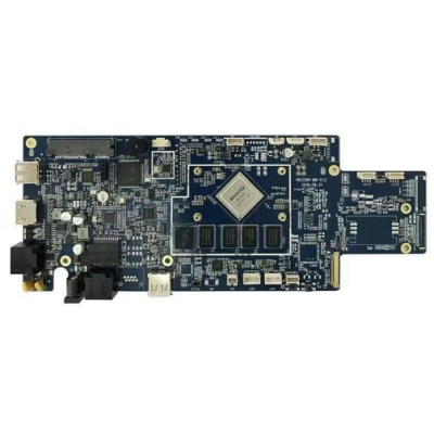
High-density compute board
AI vision products in our factory use dense compute boards related to the UAV and industrial platform families. We describe assembly capability only — board parameters are defined by your design and confirmed in the file review.
See mainboard platforms →Test Plan
Batch-level COC records follow IQC, IPQC and OQC on every lot.
X-Ray
BGA void rate below 15% verified on hidden solder joints.
ICT + FCT
Checks assemblies and functional behaviour of the vision board.
Aging test
Powered screening for devices that stay active for long periods.
Delivery & Documentation
Assembly runs in the 2,600㎡ Shenzhen facility with a factory yield of 99.7% or higher under ISO9001:2015. NDA protection and batch-level COC are standard for vision programs. Send your files to yun@dhc-pcba.com for a 24–48 hour response.
Quote an AI vision board
24–48h response · NDA on request · BOM/Gerber by email.